Bifur-circuits: Interactive and Modular Metamaterial Building Blocks Via Bifurcated Geometries
Summary: Bifur-circuits is a mechanically and electrically modular 3D metamaterial assembly toolkit that enables interactive geometries capable of exponentially increasing topological configurations through mechanical bifurcation. By embedding conductive logic and recursive node sensing into auxetic structures, Bifur-circuits allows real-time state detection across dynamic applications ranging from adaptive tangible interfaces to shape-changing spatial environments.
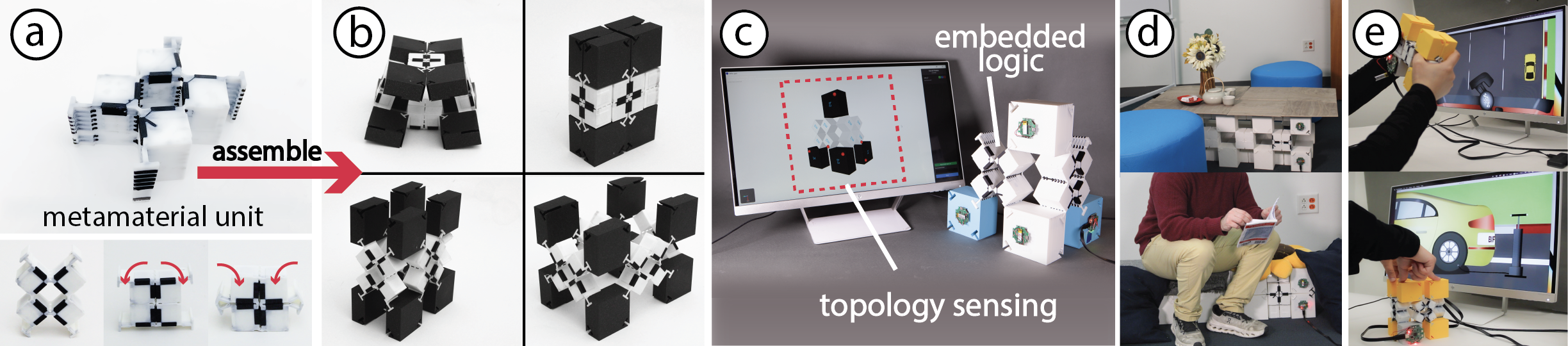
Figure 1. (a) A base metamaterial unit has three default states. (b) When bifurcated within an assembly, it exhibits multiple topology reconfigurations across a single structure. (c) Embedding electrical logic enables real-time sensing of these reconfigurations, enabling dynamic applications such as shape-changing furniture (d) and tangible user interfaces (e).
Publication Details:
Authors: Marwa AlAlawi, Regina Zheng, Abdullah Negm, Jiaji Li, Emma Li, Yasuaki Kakehi, Yoshihiro Kawahara, Junyi Zhu, Ticha Sethapakdi*, Stefanie Mueller*
Conference: In Proceedings of UIST'26
Media: Video
Mechanical metamaterials have gained traction in the HCI community for enabling interactive applications, including shape-changing displays and novel sensing paradigms. However, these structures typically support a limited set of stable geometric configurations, constraining the range of geometric expressions they can support through modularity. To overcome this constraint, we present Bifur-circuits, a mechanically and electrically modular, fully 3D metamaterial assembly toolkit.
Bifur-circuits enables interactive geometries capable of exhibiting an exponentially increasing number of configurations as a function of units in an assembly. It accomplishes this through two layers of mechanical reconfiguration:
- Assembly level: Modules can be added or removed.
- Configuration level: Structures split into new stable configurations upon reaching a critical geometric threshold via mechanical bifurcation.
All units are internally routed such that electrical modularity produces a valid and unique circuit per configuration. We contribute a Fusion 360-based construction tool, a Java-C++ simulation tool for real-time shape recognition, and a multi-material 3D printing fabrication pipeline.
Key Takeaways
- Exponential Configuration Scaling: While traditional metamaterial units have a fixed number of states, mechanical bifurcation allows the number of geometric configurations to scale exponentially ($N \propto 3^{m \times n \times p}$) with the number of units.
- Embedded Mechanical & Electrical Modularity: Internally routed conductive paths and rotationally symmetric 8-patch contact points eliminate external wiring, enabling continuous logic state sensing and recursive I2C node topology discovery.
- Robust Endurance & Linear Scalability: Technical evaluations demonstrate that 3D-printed conductive hinges maintain electrical connectivity past 10,000 cyclic compressions, with topology-discovery latency scaling linearly ($O(n)$) as units are added.
Detailed Overview
Introduction & Motivation
Conventional metamaterial structures cannot be mechanically modified after fabrication; once built, they cannot be reprogrammed without redesigning and refabricating the material. Existing modular solutions are often restricted to 2D/2.5D construction, depend on multi-step manual fabrication, or lack embedded electrical capabilities.
Where electrical modularity exists, it frequently separates mechanical structures from electronic components. This separation forces geometric reconfiguration and electrical logic to remain mutually exclusive, requiring physical disassembly and rewiring to adapt to new shapes. Bifur-circuits bridges this gap by co-designing mechanical deformation and electrical connectivity into a single unified building block.
+-----------------------------------------------------------------------+
|                             Bifur-circuits                            |
|                                                                       |
|  +---------------------------------+ +------------------------------+ |
|  |     Assembly-Level Modularity   | | Configuration-Level Bifurcat.| |
|  |  (Add / Remove 3D Building Blks)| | (Split into stable shapes)  | |
|  +---------------------------------+ +------------------------------+ |
|                                  |                                    |
|                                  v                                    |
|              +---------------------------------------+                |
|              |  Embedded Conductive Logic & Circuits  |                |
|              +---------------------------------------+                |
|                                  |                                    |
|                                  v                                    |
|              +---------------------------------------+                |
|              |    Real-Time Topology Recognition     |                |
|              +---------------------------------------+                |
+-----------------------------------------------------------------------+
Bifur-circuits Working Principle
Construction Principle
Bifur-circuits structures consist of two primary building block geometries:
- Metamaterial Units: Auxetic kirigami structures made of non-conductive materials internally routed with conductive traces.
- Connector Blocks: Rigid blocks used to interlock metamaterial units. These come in two types: Type AB (orthogonal, for corners/depth) and Type C (co-linear, for linear 2D expansion).
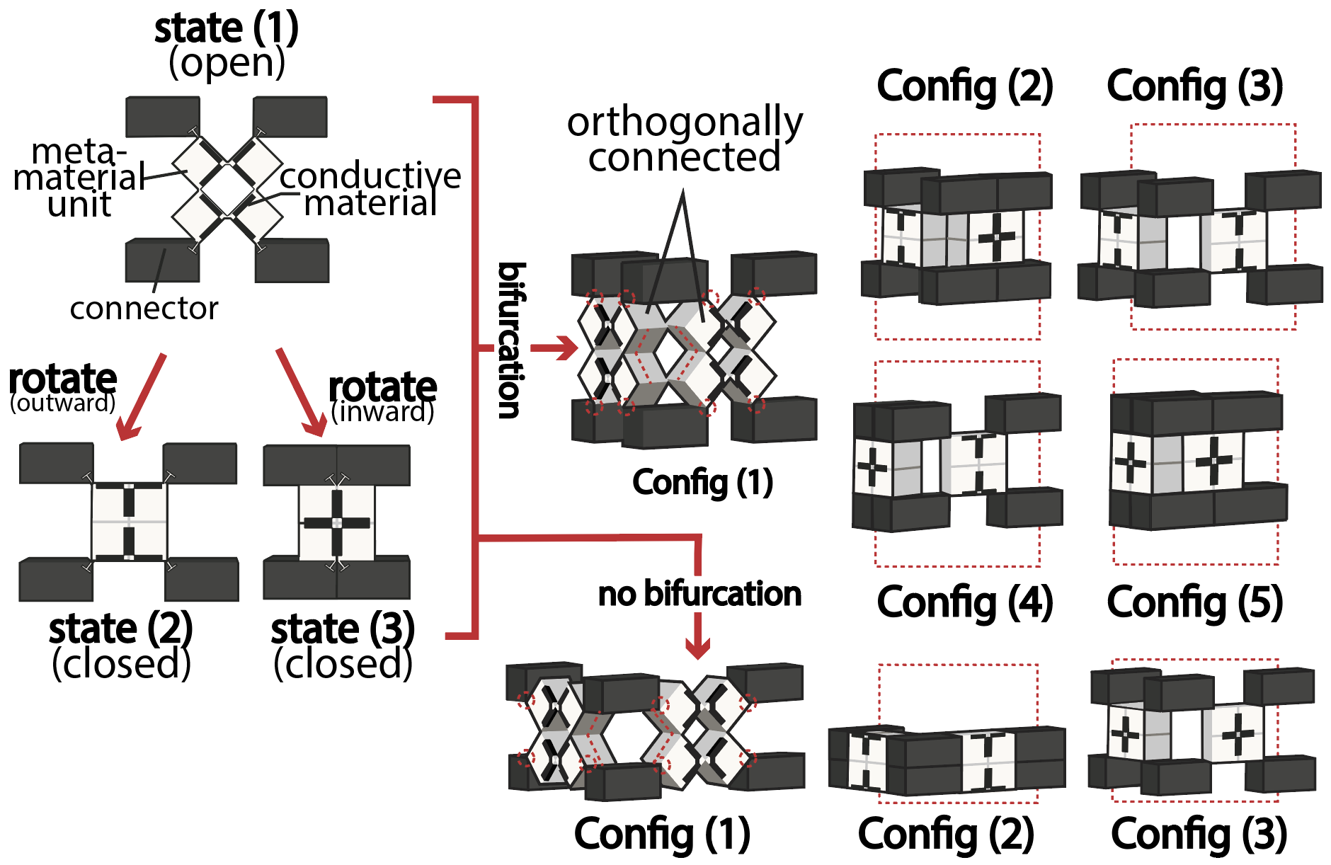
Figure 2: A single metamaterial unit has three states; bifurcation yields multiple assembly configurations.
Assemblies are formed by press-fitting metamaterial units and connector blocks. A single auxetic unit exhibits three default states due to rotation (State 1: open, State 2: closed, State 3: closed). By linking units adjacently or perpendicularly (bifurcation), the available configuration space scales exponentially.
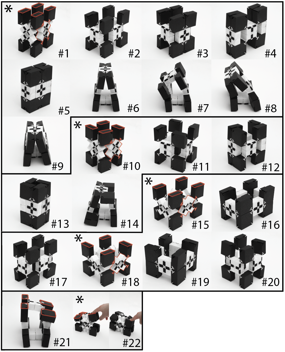
Figure 3: A 2×2×1 assembly yielding 22+ configurations: groups (1–9) and (10–14) share the same structure within each group but differ in connector orientation between groups; 15–20 are non-bifurcated reconfigurations; 21–22 demonstrate asymmetric connector orientations.
Sensing Principle
Conductive material is applied directly to the inner edges of the metamaterial unit that come into contact when transitioning between states. Touching edges close a unique circuit corresponding to that unit's state.
Each connector block contains four connection ports with independent Data (SDA) and Clock (SCL) lines. A designated "root" node initiates a scan across its ports, requesting node IDs and connection topologies from neighboring units recursively via downstream I2C masters. This process builds a JSON connection map representing the assembly's global physical shape.
Designing Bifur-circuits
Design Parameters
The physical properties and state count of a Bifur-circuit assembly are dictated by four primary parameters:
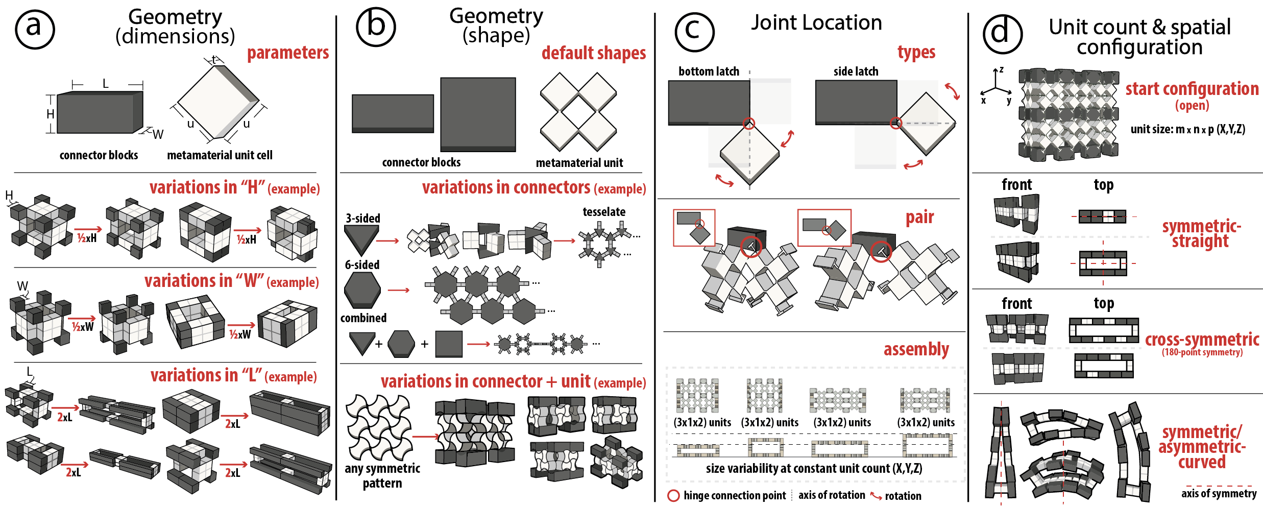
Figure 4: Design parameters of Bifur-circuits. (a) Connector block and unit cell dimensions, parameterized by H, W, L, u, and t. (b) Default and variant connector/metamaterial geometries. (c) Joint location through bottom and side latch types across varying X, Y, Z sizes. (d) Spatial configurations — symmetric, cross-symmetric, and asymmetric — across grid sizes (m×n×p).
- Geometry (Dimensions & Shape): Parameterized by connector height ($H$), length ($L$), width ($w$), and metamaterial thickness ($t$) and unit square length ($u$).
- Joint Location: Units connect to blocks at vertices using either a bottom-latch (45° angle relative to block length) or side-latch (45° angle relative to block height) orientation.
- Unit Count: Total theoretical geometric configurations follow the proportion: $N(m, n, p) \propto 3^{m \times n \times p}$ where $m$, $n$, and $p$ represent unit counts along the X, Y, and Z axes.
- Unit Stability: Governed by the equilibrium between elastic hinge springback forces and magnetic attraction. Units can be configured to be monostable (returning to default open state) or bistable/tristable (holding shapes via embedded N45 Neodymium magnets).
Design Space
The system spans three dynamic axes: Form (1D, 2D, and 3D solid/hollow structures), Compliance (fully rigid, fully elastic, or spatially varying), and Interaction (compression, stretching, rotation, and bending).
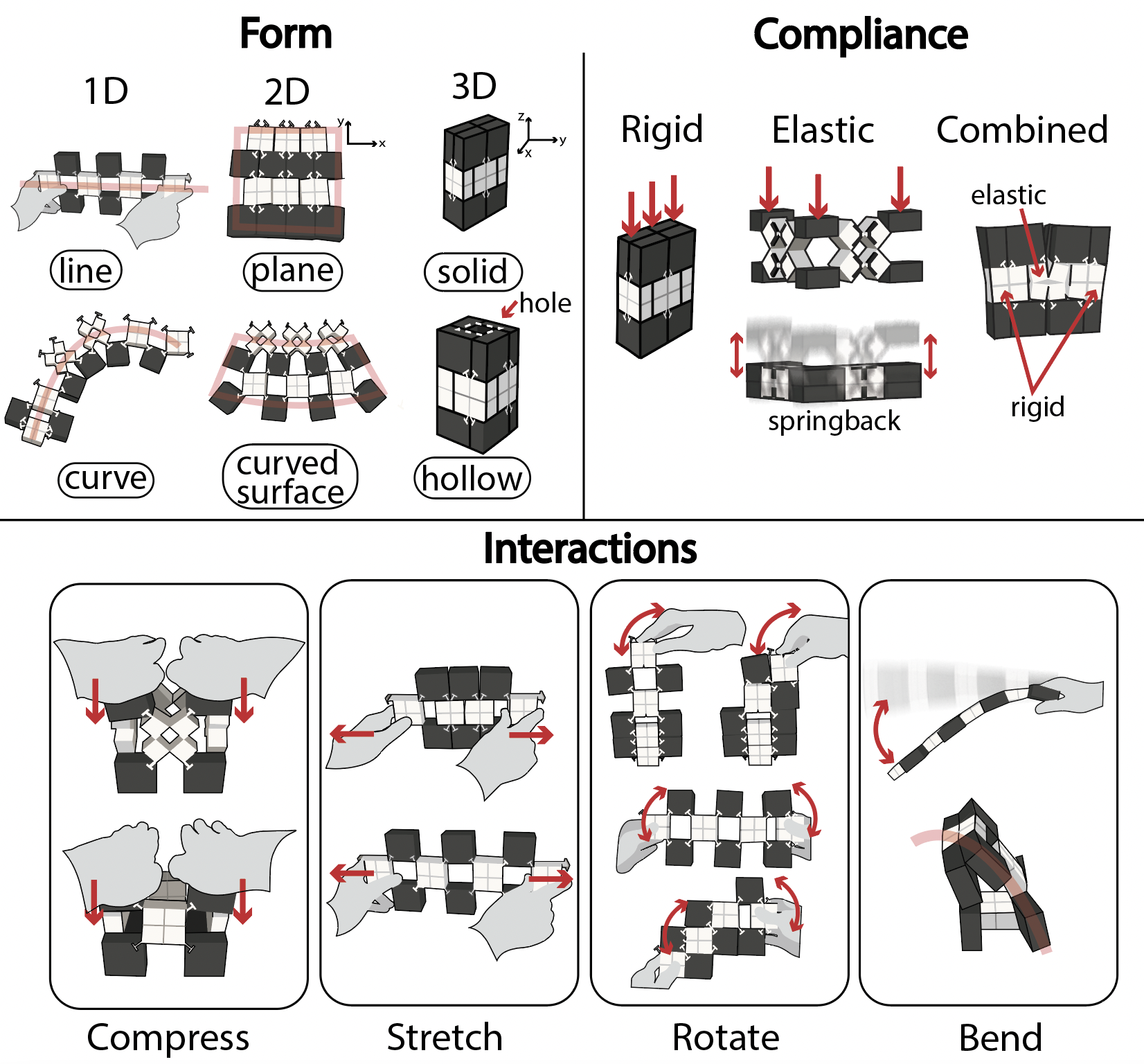
Figure 5: Bifur-circuits design space organized along three parameters: form, compliance, and interaction.
Modular Mechanical & Electrical Architecture
To satisfy strict modular requirements (tool-less assembly along XYZ, secure detachable joints, and valid electrical continuity under strain), the physical design incorporates several features:
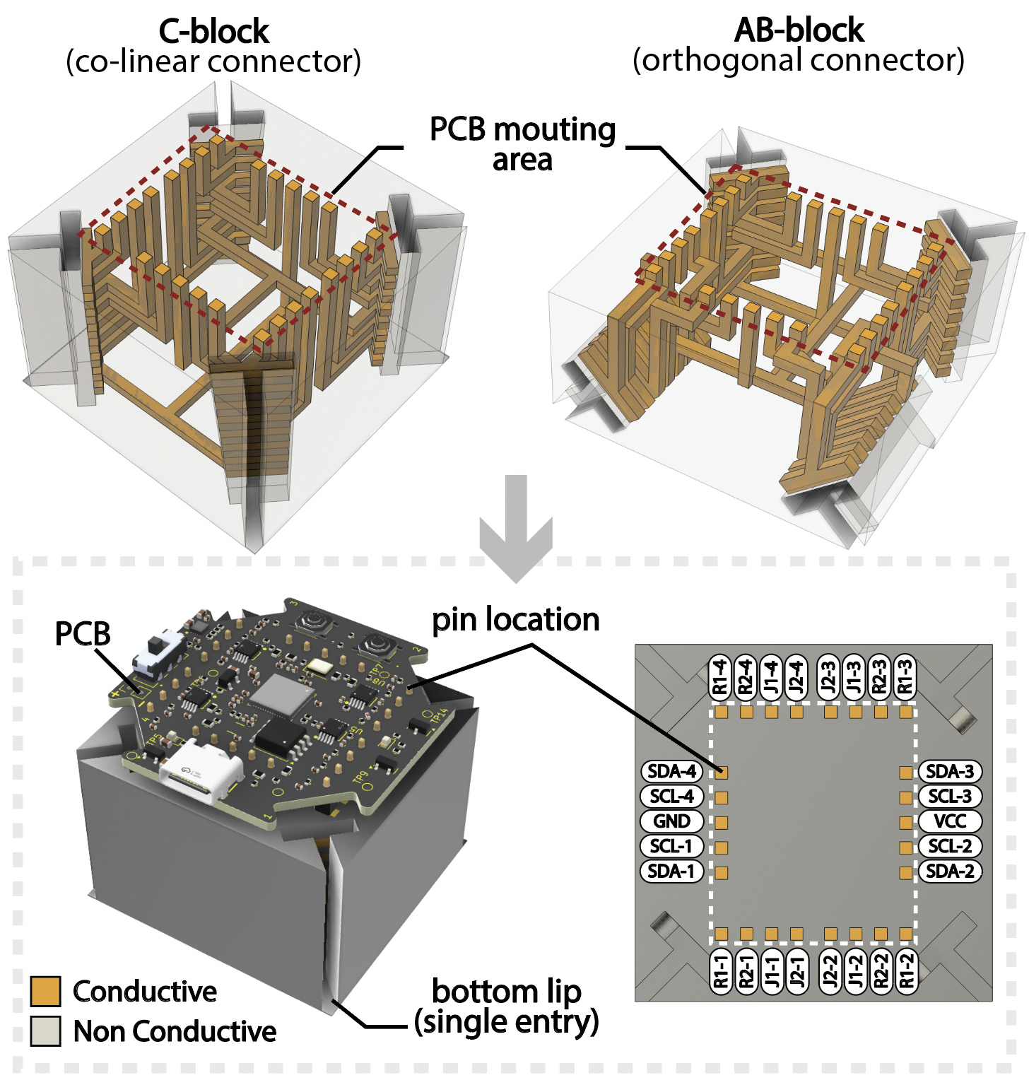
Figure 6: The two connector block variants (Types AB and C) are internally routed with conductive material and interface with a top-mounted PCB.
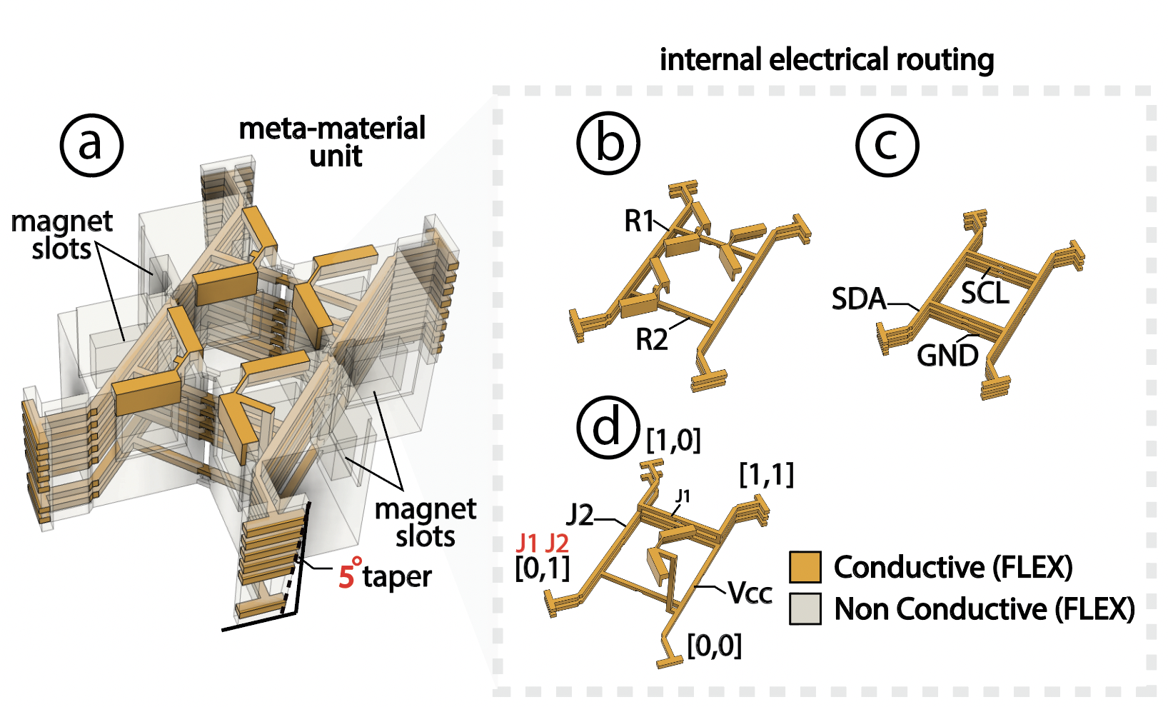
Figure 7: Metamaterial unit structure and internal electrical routing.
- Angled T-Joint Connections: Prevents accidental disengagement while co-locating attachment entry points directly at vertex axes.
- 5° T-Joint Taper & Sealed Single Entry: Enforces single-orientation insertion to prevent inverse electrical connections.
- Rotational Symmetry: Each successive T-joint is rotated 90° to enable flexible hinge placement while keeping electrical pin polarity aligned.
- 8-Patch Contact Arrays: Connection points feature 8 conductive patches (VCC, J2, J1, GND, SCL, SDA, R1, R2). Joint logic pins (J1/J2) differ across joints to encode physical insertion orientation.
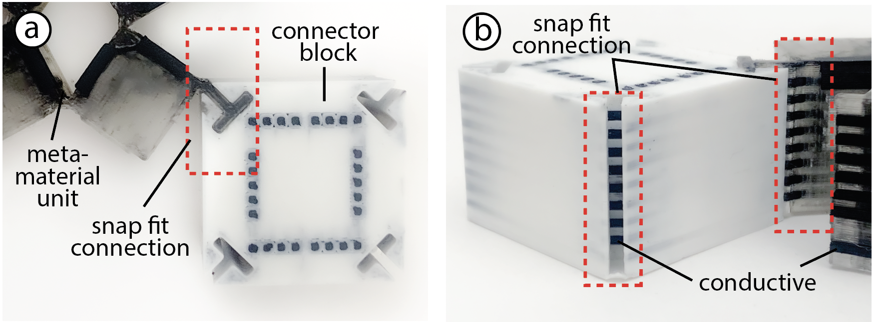
Figure 8: Metamaterial units and connectors attach mechanically and electrically through a snap fit connection.
Deep Dive & Technical Insights
Fabrication & Interaction Pipeline
Fusion 360 Construction Tool
A custom add-in allows users to input geometric dimensions (minimum unit size: 20 mm, thickness: 28 mm) and desired stability modes. Monostable and tristable selections automatically generate pockets for magnet insertion spaced 1 mm from interior walls.
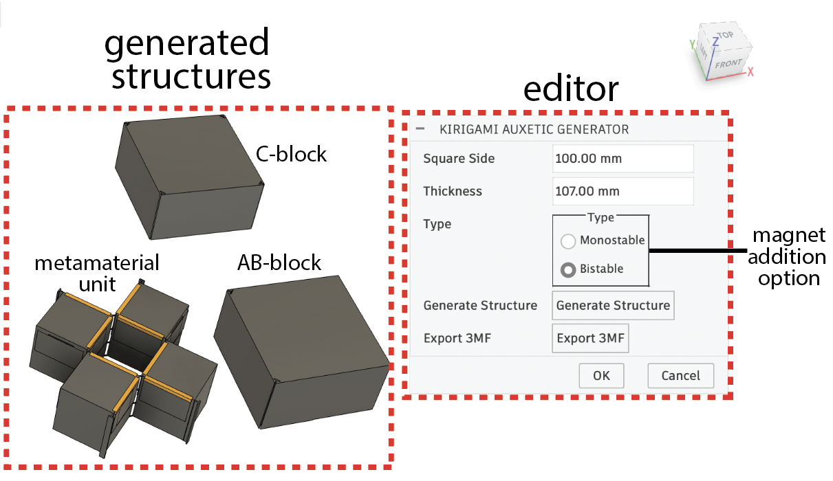
Figure 9: The Bifur-circuit Editor allows users to generate metamaterial units and connector blocks.
Multi-Material 3D Printing
- Metamaterial Units: Fabricated via multi-material FDM using flexible conductive TPU (Filaflex 92 A, 100% infill, 99 perimeters) for circuit traces/hinges and non-conductive TPU (SainSmart 95 A, 15% infill) for main structural bodies. Printing pauses mid-process to insert N45 Neodymium magnets ($3/8 \times 3/8 \times 1/8\text{ inch}$).
- Connectors: Printed using rigid PLA bodies with embedded Filaflex conductive channels.
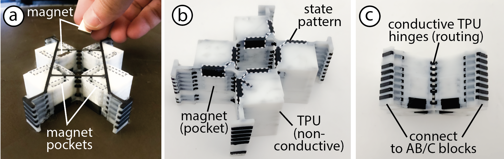
Figure 10: Bifur-circuit metamaterial unit fabrication. (a) Embedding magnets mid-print. (b) Unit in open state displaying TPU body, conductive patches, and magnet pockets. (c) Close-up of flexible conductive hinges.
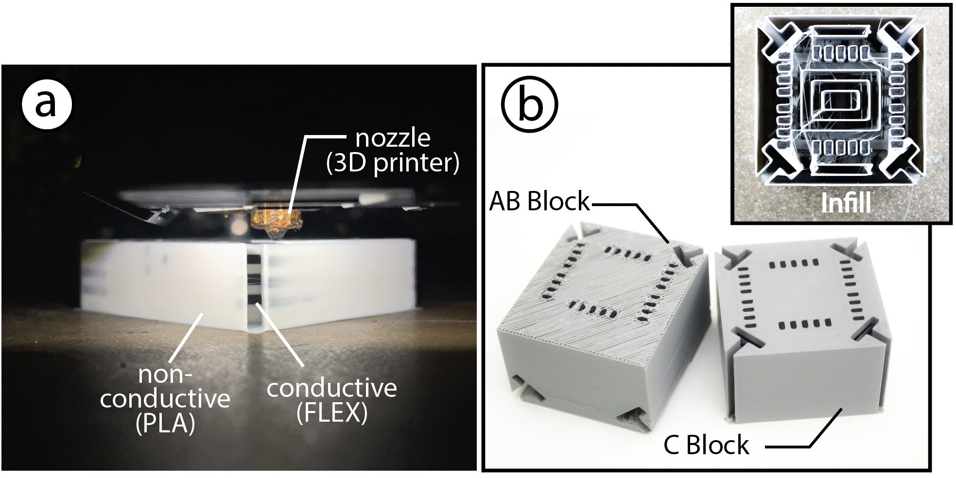
Figure 11: (a) AB and C connector blocks are multimaterial 3D printed (TPU and conductive FLEX material) with a concentric infill (b).
PCB Assembly & Interaction Authoring
Custom PCBs featuring RP2040 microcontrollers are heat-pressed and soldered directly onto the conductive patches of connector blocks.
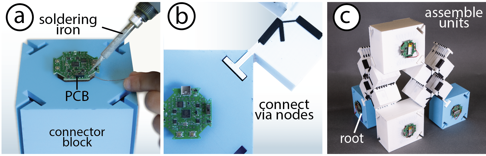
Figure 12: (a) PCB mounted on connectors via heat press and soldering. (b) Connectors attach to metamaterial units to form assemblies (c).
An interactive Java/Processing UI displays live 3D assembly visualizations, allows users to save named topological states, and exports generated C++ libraries for interaction mapping.
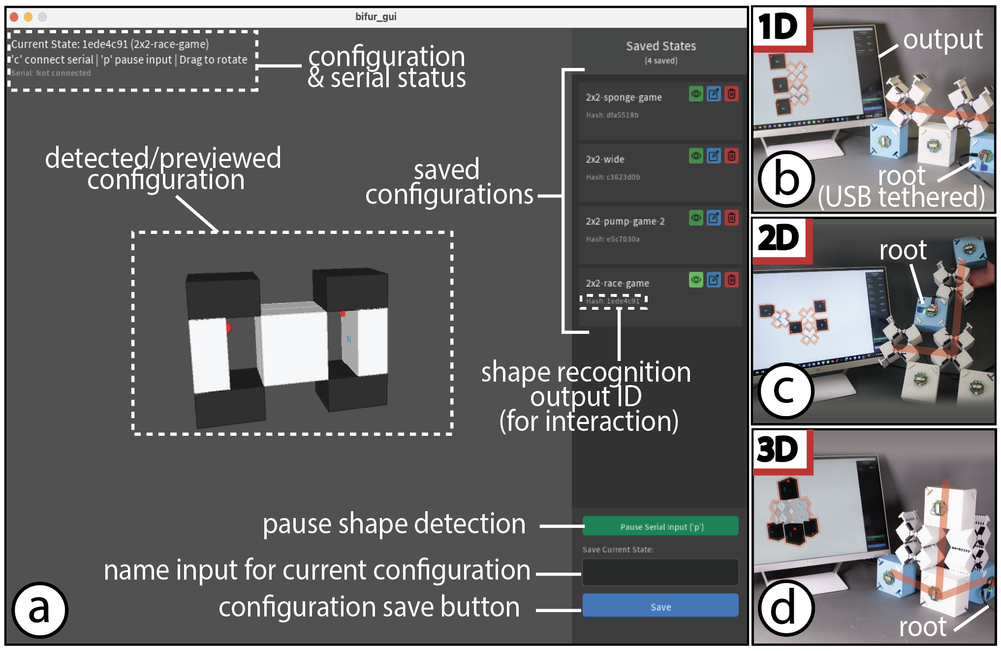
Figure 13: (a) Bifur-circuit UI detects & saves 1D (b), 2D (c), and 3D topologies (d).
Technical Evaluation
Latency as a Function of Unit Count
To test topology-discovery scaling under material resistance constraints, 20 Bifur-circuit PCBs were daisy-chained with $27\text{ k}\Omega$ inter-node resistances (representing worst-case trace resistance).
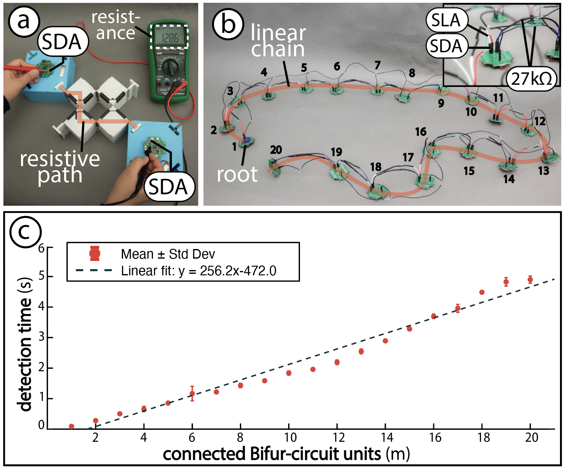
Figure 14: (a) Resistance measurement of longest SDA path between neighboring connectors, (b) linear chaining setup of PCBs, and (c) resultant latency performance.
| Measured Ports | Largest Unit Resistance | Smallest Unit Resistance |
|---|---|---|
| SDA ($\Omega$) | $13.08 \pm 0.80\text{ k}\Omega$ | $15.215 \pm 0.2549\text{ k}\Omega$ |
| SCL ($\Omega$) | $12.09 \pm 1.91\text{ k}\Omega$ | $17.001 \pm 0.2309\text{ k}\Omega$ |
Table 1: Measured I2C line resistances across 10 samples for extreme element sizes.
Latency ($t$) follows a linear relationship ($R^2 = 0.9727$) relative to unit count ($m$), consistent with $O(n)$ recursive I2C discovery: $t_{\text{detection}} = 256.2 \times m - 472 \quad (\text{in ms})$ A chain depth of 20 units yields a total detection latency of approximately 5 seconds.
Electrical Connectivity Endurance
A texture analyzer subjected conductive TPU hinges to 10,000 compression cycles under three configurations: cyclic loading along axis 1, cyclic loading along axis 2, and alternating reverse cyclic loading.
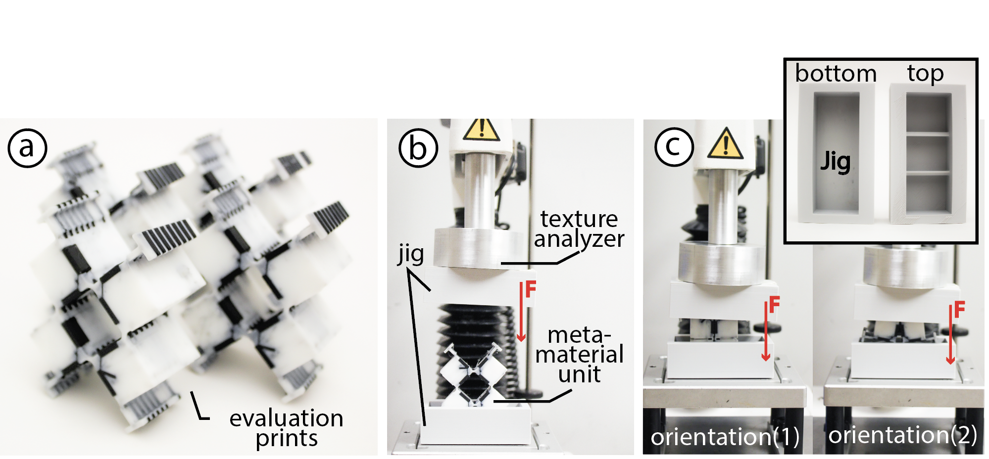
Figure 15: (a) Metamaterial units with conductive routing for (b,c) cyclic and reverse cyclic compression tests using a texture analyzer load cell.
Results: All samples retained continuous electrical conductivity across 10,000 complete rotations without structural tearing or trace degradation.
Application Domains
1. Programmable Spatial Environments
A human-scale architectural assembly comprising 24 metamaterial units and 24 blocks ($40\text{ cm} \times 30\text{ cm} \times 110\text{ cm}$) reconfigures dynamically into three distinct furniture modes while updating a connected digital door display:
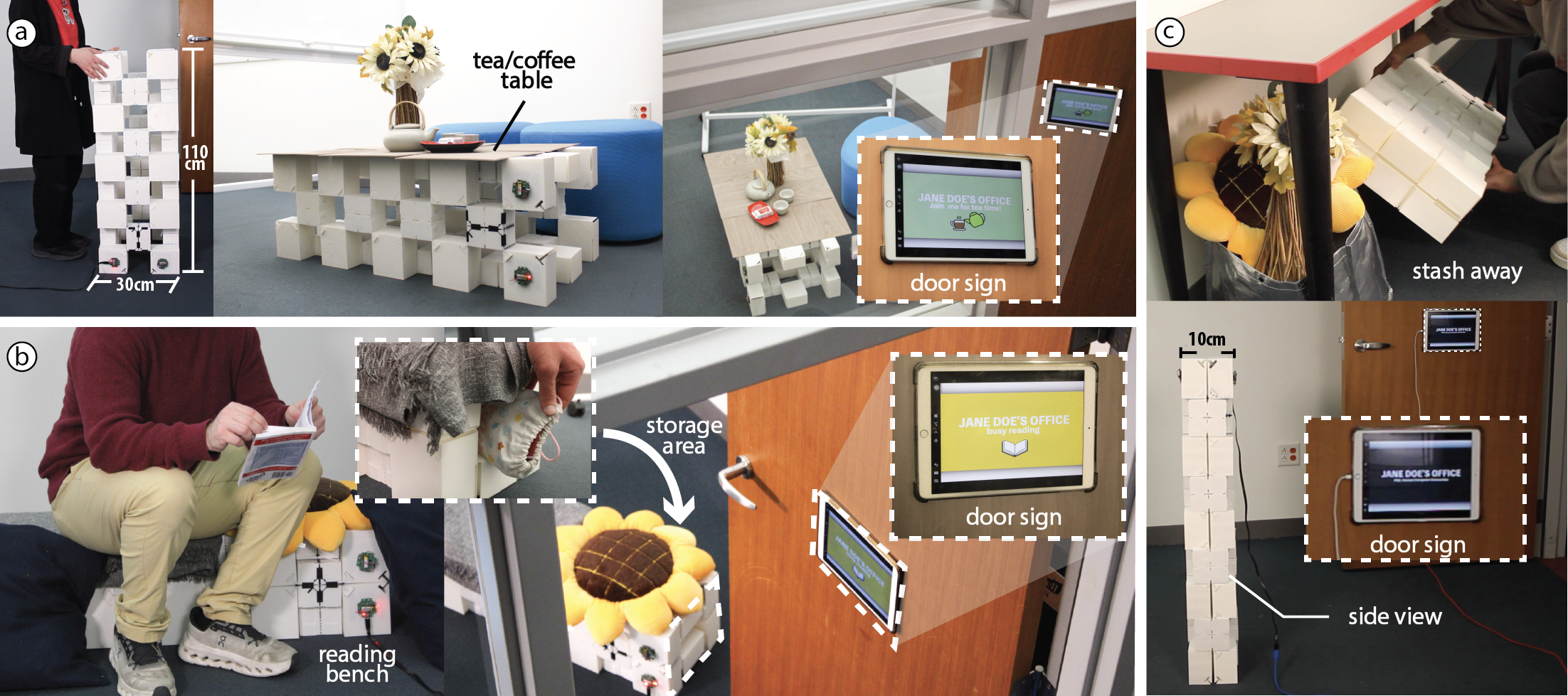
Figure 16: Human-scale reconfigurable furniture application. (a) Fully expanded into a tea table (Door sign: "Welcome"). (b) Retracted with opening into a reading bench (Door sign: "Busy reading"). (c) Fully collapsed flat for storage.
2. Reconfigurable Tangible User Interfaces
A single 4-unit Bifur-circuit structure functions as a multi-modal game controller, shifting between functional physical roles without requiring auxiliary attachments:
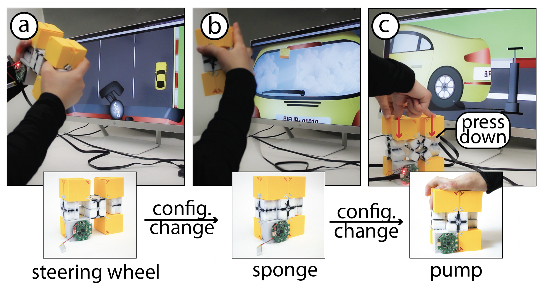
Figure 17: Four Bifur-circuit configurations acting as a shape-changing game controller triggering: (a) racing wheel mode, (b) sponge/car-wash mode, and (c, d) pumping tire inflation mode.
Discussion & Future Work
- Shape Memory Tuning: TPU's viscoelastic properties introduce a directional bias toward recently held shapes. This bias persists for over 12 hours and can be re-programmed manually.
- Power Distribution: Due to material resistivity ($3.9,\Omega\cdot\text{cm}$), traces experience voltage drop across large assemblies. Power is currently distributed using localized $62\text{ mAh}$ LiPo batteries per node. Future iterations will incorporate super-conductive flexible materials to enable centralized power routing.
- Selective Node Sensing: Latency can be improved by replacing redundant microcontrollers with passive buffer blocks and sensing only minimal state-resolving paths.
Conclusion & Resources
Bifur-circuits introduces a combined electro-mechanical framework for 3D metamaterial design. By leveraging mechanical bifurcation alongside embedded, wire-free conductive routing, the system converts auxetic units into scalable, state-aware building blocks.
- Key Takeaway: Merging mechanical bifurcation with embedded electrical logic expands the reconfigurable state space from static 3-state units to an exponentially scalable $3^{m \times n \times p}$ matrix.
- Design Toolkit: Includes Fusion 360 CAD generation tools, Java/Processing state management software, and an FDM multi-material fabrication workflow.
References
- Stephan Hankammer, Ruth Jiang, Robin Kleer, and Martin Schymanietz. 2016. From phonebloks to google project ara. Procedia CIRP.
- H MA Kolken, and AA Zadpoor. 2017. Auxetic mechanical metamaterials. RSC Advances.
- Ken Nakagaki et al. 2016. ChainFORM: A Linear Integrated Modular Hardware System for Shape Changing Interfaces. ACM UIST.
- Yanbin Li, Caizhi Zhou, and Jie Yin. 2024. Geometric mechanics of kiri-origami-based bifurcated mechanical metamaterials. Philosophical Transactions of the Royal Society A.
- Jun Gong, Olivia Seow, Cedric Honnet, Jack Forman, and Stefanie Mueller. 2021. MetaSense: Integrating Sensing Capabilities into Mechanical Metamaterial. ACM UIST.
- Kaili Xi et al. 2025. A Kinematically Bifurcated Metamaterial for Integrated Logic Operation and Computing. Advanced Science.
- Alexandra Ion, Ludwig Wall, Robert Kovacs, and Patrick Baudisch. 2017. Digital Mechanical Metamaterials. ACM CHI.